Custom OEM ODM Prototype PCB Assembly Service LED Lighting industry
2PCS
MOQ
large.img.alt
Features Gallery Product Description Request A Quote
Features
Basic Infomation
Place of Origin: China
Brand Name: Yizhuo
Certification: CE,ROHS,UL
Model Number: led pcb assembly 01
High Light:

ODM Prototype PCB Assembly

,

OEM Prototype PCB Assembly

,

ODM PCB Fabrication Service

Payment & Shipping Terms
Packaging Details: Inner vacuum packing,Outer standard carton box packing.
Delivery Time: 10-12 work days
Payment Terms: T/T, Western Union
Specifications
Product Name: Oem Led Light Pcba
Led CCT: 3000k-6500k,630nm, 660nm,730nm
PCB Assembly Test: Visual Inspection (default), AOI, FCT
Surface Finishing: HASL / OSP / ENGING
PCB Assembly Method: SMT, Through-hole, Mixed
Testing Service: Fly-probe,100% AOI Testing, 100% ET Testing
Product Description

Custom OEM ODM Prototype PCB Assembly Service LED Lighting Industry


Led pcb board aluminum circuit boards custom service pcb manufacturers


Aluminum PCB: 

Aluminum PCB is a kind of metal-based copper clad laminate with good heat dissipation function. Generally, single panel consists of three layers, namely circuit layer (copper foil), insulation layer and metal base. Used for high-end use is also designed for double panels, the structure is circuit layer, insulation layer, aluminum base, insulation layer, circuit layer. Very few applications are multi-layer boards, which can be made by bonding ordinary multi-layer boards with insulating layer and aluminium base.

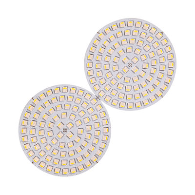
LED PCB is Aluminum PCB, which is also the meaning of printed circuit board, but the material of PCB is aluminum alloy. In the past, the material of PCB is glass fiber, but because the heat of LED is bigger, the PCB used for LED lamps is generally aluminum Substrate, which can conduct heat quickly. The PCB used for other equipment or electrical appliances is glass fiber board.


Structure of aluminum PCB
PCB aluminum based copper clad laminate is a kind of metal circuit board material, which is composed of copper foil, thermal insulation layer and metal substrate


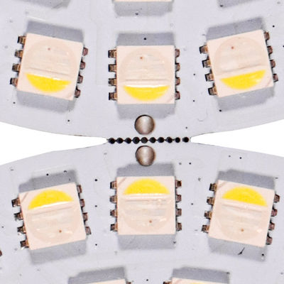
1. Circuit layer: equivalent to common PCB copper clad laminate, circuit copper foil thickness from 1oz to 10oz.


2.  Insulating layer: insulating layer is a layer of low thermal resistance thermal insulation material. Thickness: 0.003 "to 0.006" inch is the core technology of aluminum based copper clad laminate, which has obtained UL certification.


3.  Base: is a metal substrate, generally aluminum or optional copper. Aluminum based copper clad laminates and traditional epoxy glass cloth laminates


PCB aluminum substrate is composed of circuit layer, thermal insulation layer and metal base layer; circuit layer (i.e. copper foil) is usually etched to form printed circuit, so that the components of components are connected with each other. Generally, the circuit layer requires a large current carrying capacity, so thick copper foil should be used, with a thickness of 35 μ m ~ 280 μ M. Thermal insulation layer is the core technology of PCB aluminum substrate. It is generally composed of special polymer filled with special ceramics. It has small thermal resistance, excellent viscoelastic performance, thermal aging resistance, and can withstand mechanical and thermal stress. This technology is used in the thermal insulation layer of High Performance PCB aluminum substrate, such as IMS-H01, IMS-H02 and LED-0601, which makes them have excellent thermal conductivity and high strength electrical insulation performance.


Metal base is the support component of aluminum substrate, which requires high thermal conductivity. Generally, aluminum plate can be used, and copper plate can be used (copper plate can provide better thermal conductivity), which is suitable for drilling, punching, cutting and other conventional machining. Compared with other materials, PCB material has incomparable advantages. Suitable for SMT technology of power module surface mounting. Without radiator, the volume is greatly reduced, the heat dissipation effect is excellent, and the insulation and mechanical properties are good.


No.

Item

Specification

1

PCB Layers

1 to 24 layers

2

PCB Max working panel area

457 x 610 mm

3

Min trace width

0.10mm

4

Min spacing

0.10mm

5

Min hole diameter

0.20mm

6

Min Copper thickness in hole

0.020mm

7

PTH size tolerance

±0.05mm

8

NPTH size tolerance

±0.025mm

9

Hole position tolerance

±0.05mm

10

Dimension tolerance

±0.1mm

11

Min solder mask dam

0.08mm

12

Insulation resistance

1E+12Ω (normal condition)

13

Max Board twist and wrap

≤0.7%

14

High Vlotage endurance

1.3KV/mm

15

Copper foil peel off endurance

1.4N/mm

16

Hardness of resist ink

≥6H

17

Flame resistance

94V-0

18

Impedance control

±5%


Custom OEM ODM Prototype PCB Assembly Service LED Lighting industry 0

Custom OEM ODM Prototype PCB Assembly Service LED Lighting industry 1

 
FAQ: 


Q1.  How to deal with the faulty?

A:  Firstly, Our products are produced in strict quality control system and the defective rate will be less than 0.1%. Secondly, during the guarantee period, if it's our fault, we will repair them and resend to you or we can discuss the detail, and find the final solution.


Q2:  Is it OK to print my logo on product?

A:  Yes. Please inform us formally before our production and confirm the design firstly based on our sample.


Q3:  Do you offer guarantee for the products?

A:  Yes, we offer 2 years warranty to our products.

Recommended Products
Get in touch with us
Contact Person : Yolanda Yao
Tel : +8613430550241
Fax : 86-755-33115535
Characters Remaining(20/3000)