
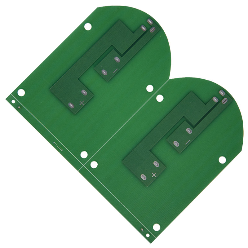
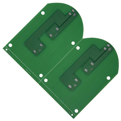
Aluminum Base PCB Gold Plated 2oz Copper Printed Circuit Board
![]()
![]()
PCB PRODUCTION CAPACITY
| PCB layers | 1-layer to 10-layer(including HDI board) |
| Finish type | Gold-plated,Immersion gold-plated, HAL finish , Flux., Carbon -bridge, Entek, Nickel plating |
| Base material | FR4,CEM-1,CEM-3,FR1,FR2, Aluminium metal substrate and Rogers |
| Base material thickness | 0.4-2.4mm. |
| Copper foil thickness | 18um(H/HOZ) ,35um(1/1OZ) ,70um(2/2OZ), 5OZ |
| Maximum-product board | 500*700mm. For AL PCB: 500*1400mm |
| Minimum drilled hole size | 0.075mm |
| Minimum track width/spacing | 3mil |
| Average hole wall copper | Thickness for HAL board: ≥25um.Gold-finger plating: ≥0.1um |
| Solder mask ink | Photo cure ink, heat cure ink. UV ink |
| Outline tolerance | ±0.1mm |
| Hole diameter tolerance/ Hole location tolerance | ±0.076mm/±0.076mm |
| V-CUT tolerance | ±0.1mm. |
| Warp | According to the IPC-600F standard |
| lead time | Single-sided: 2-3 working days; Double-sided: 3-4 working days; Multi-layer: 8-10 working days |
PCBA MANUFACTURING CAPABILITY
| PCB assembly Layers | 1 Layer to 36 layers (standard), |
| PCB assembly material/type | FR4, Aluminum, CEM1, Super-thin PCB, FPC/Gold finger |
| PCB Assembly service type | DIP/SMT or Mixed SMT & DIP |
| Copper thickness | 0.5um-4um |
| Assembly surface finish | HASL,ENIG,OSP |
| PCB Dimension | 600x1200mm |
| IC Pitch(min) | 0.2mm |
| Chip Size(min) | 01005 |
| Leg distance(min) | 0.3mm |
| PCB BGA Size | 8x6mm~55x55mm |
| IC Encapsulation type | SOP/CSP/SSOP/PLCC/QFP/QFN/BGA/FBGA/u-BGA |
| u-BGA ball dia. | 0.2mm |
| Required Docs for PCBA | Gerber file with BOM list & Pick-N-Place File(XYRS) |
| SMT speed | CHIP components SMT speed 0.3S/pcs, max speed 0.16S/pcs |


