
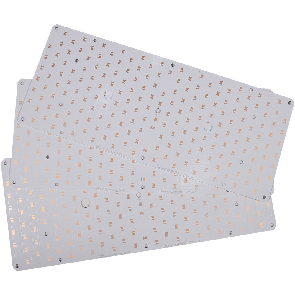
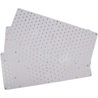
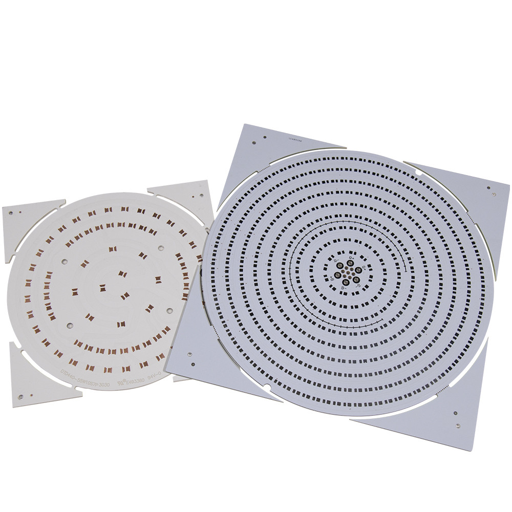
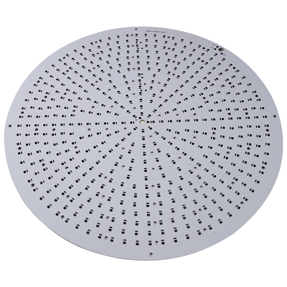
Single-sided aluminium 94vo led pcb copper base PCB for lighting
Custom Single Sided 94V0 Copper Base PCB Lead Free HASL FinishingCustom Single Sided 94V0 Copper Base PCB Lead Free HASL Finishing
| Substrates Material | Aluminum |
| Board thickness | 0.6- 3.0mm |
| Copper Foil thickness | 0.5oz- 6oz |
| Surface treatment | HAL/OSP/Immersion Gold Plating/Gold Plating/Sn Plating/Immersion Sn |
| Thermal Conductivity | 1.0- 3.0W/m.k |
| Breakdown Voltage | 2-4.5KV |
| Combustibility | 94V0 |
| Services | OEM&ODM |
| Standard | UL&ROHS |
Aluminum PCB performance:
1. Heat dissipation
Compared to normal FR4 PCBs, the aluminum PCBs perform better and more quickly in heat dissipation. Take the FR4 PCB and the aluminum PCB with the same thickness of 1.5mm as an example. FR4 PCBs have a thermal resistance of from 20°C/W to 22°C/W while aluminum PCBs have it of from 1°C/W to 2°C/W, which proves the feature again.
2. Thermal expansion
The thermal expansion and contraction are common properties of substances but have different coefficients. Because of the excellence in heat dissipation of the aluminum PCBs, the problems on the thermal expansion and contraction on the board surface will be significantly reduced to increase the durability and reliability of the entire equipment and electronic devices. This kind of advantages can be particularly suitable for the thermal expansion and shrinkage problems of surface mount technology (SMT).
3. Dimensional stability
The aluminum PCBs have significantly stable dimensions. Their dimensions will only change about 2.5% to 3.0% when they are heated from 30 ℃ to 140 ℃ or even 150 ℃.
4. Other performance
a. Applicability to power device SMT.
b. Effective thermal expansion of circuit design.
c. Helpful to reduce operating temperature, improve product power density and reliability, and extend the shelf life of products.
d. Helpful to reduce the size of the product, hardware and assembly costs.
e. Easy replacement of fragile ceramic substrates with better insulation performance and mechanical durability.
![]()
![]()
Why Choose Us?
Professional PCB fabrication team -all engineers have years’ experience in PCB manufacturing field
Advanced equipment and high precision inspection & testing tools
Top raw materials including CCL (Copper Clad Lamination), chemistry, and solder mask ink & legend ink
Skilled operators with good command of all CCPs (Critical Control Points)
Full set of surface finish equipment can do ENIG, immersion silver, immersion Tin, OSP, HASL (lead free), plating gold and plating silver without outsourcing risk.
Cutting edge printed circuit board manufacturing process capacities
Max aspect ratio reaches to 10 : 1
Max copper weight on double PCB surface can reach to 6OZ
The thickness of solder mask can control to 50μm
Min Impedance control value is 50ohm +/- 5%
Min NC drilling diameter 0.2mm and min laser drilling diameter is 0.1mm
Circuit board manufacturing strictly as per IPC standards and make sure 100% qualified
Strictly perform PDCA (Plan-Do-Check Action Cycle) process, and continuously improve product performance
Leading outstanding enterprise of energy saving and environmental protection


